TCA’s 50th Anniversary Special Event – the Taiwan Semiconductor Day Forum Debuts in Tokyo on April 2
Publish Date :2024/04/02
Taipei Computer Association (TCA) is Taiwan’s largest ICT industry association with over 4000 members that contribute to over 80% of Taiwan’s ICT industry total production value. Since its establishment in 1974, TCA has developed close cooperation with the supply chains of the ICT industry. Through Taiwan’s tech industry, TCA aims to help drive the global digital transformation efforts and usher in the AI era. The TCA Japan Office was established in 1990 to promote industrial cooperation between Taiwan and Japan, assisting Taiwanese manufacturers expand into the Japanese market.
To celebrate its 50th anniversary, TCA held the Taiwan Semiconductor Day Forum in Tokyo, Japan on April 2. The event also aimed to welcome the era of inclusive AI together with both Taiwanese and Japanese industries. The forum gathered over 400 participants from Japanese industries, government, academia, and research professionals; representing many leading Japanese technology companies as well as both Japanese mainstream news outlets and Taiwanese media.
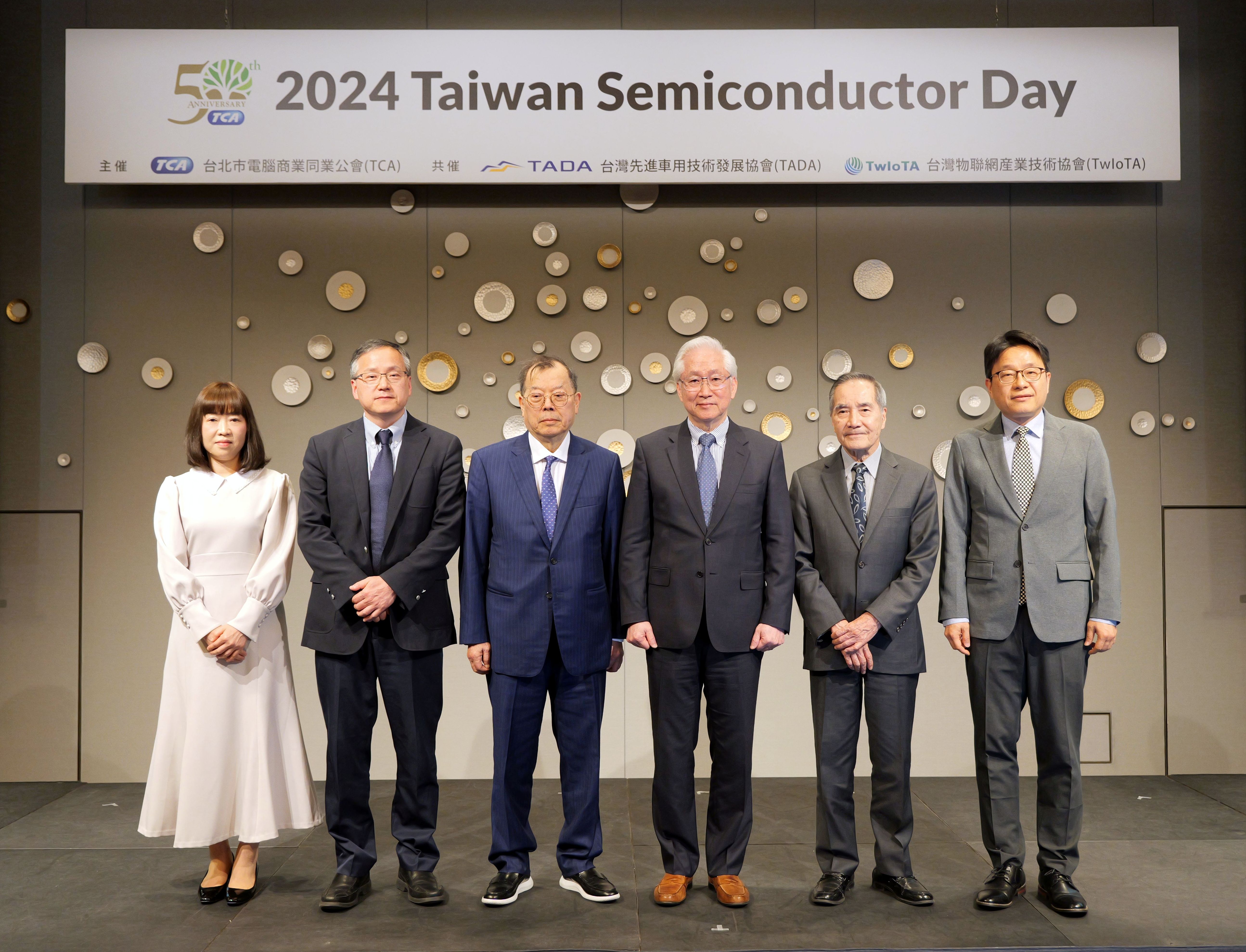
The event featured speakers representing Taiwan’s leading semiconductor manufacturers including Dr. Frank Huang, the Founder and Chairman of PSMC and chairman of Taiwan Advanced Automotive Technology Development Association (TADA); Professor Burn-Jeng Lin, the Dean of the College of Semiconductor Research in National Tsinghua University and Vice President/Distinguished Fellow of TSMC; Dr. Wen Chen, Chairman/ CEO/ CTO of AP Memory; and Hong-wen Lin, author of Chip Island: TSMC, Semiconductor and Chip War and contributing columnist for Business Week.
Wu Tsung-tsong: Taiwan and Japan are Accelerating Cooperation in Semiconductor and AI Technologies as National Science and Technology Council’s Taiwan Chip-Based Industrial Innovation Program Consolidates the Strengths of Taiwan’s Semiconductor Industry
Minister of Science and Technology Council of Taiwan, Wu Tsung-tsong said in his opening speech that with the rapid rise and development of AI and smart electric vehicles, semiconductors and AI have become the core driving force for the development of the global tech industry and become vital strategic industries for various countries. Taiwan’s semiconductor and ICT industries have played a pivotal role in the world, cooperating with partners globally to achieve mutual benefit.
The National Science and Technology Council (NSTC) is the agency responsible for promoting the development of science and technology. They focus on 3 main tasks: promoting Taiwan’s overall technological development, supporting academic research, and developing science parks. They provide the groundwork for semiconductor and ICT industries, technological research, and a strong support for the Taiwanese semiconductor industry.
Minister Wu stated that in order to continue Taiwan’s semiconductor strategic advantages, the NSTC will promote the Taiwan Chip-Based Industrial Innovation Program in 2024. The program aims to promote accelerated innovation and breakthroughs in the entire industry. The program has 4 main strategies, namely: integrate generative AI with silicon chips to drive innovation, improve domestic talent cultivation and attract global R&D professionals, accelerate adoption of heterogeneous integration and other advanced innovation technologies, and harness Taiwan's "silicon island" strengths to attract international startups and investment. This program hopes to cultivate more Taiwanese IC design startups in the next five years. Japanese industries interested in cooperating with Taiwan’s IC supply chain to expand their digital transformation business opportunities in global industries are welcome to the program.
Minister Wu also shared that in the future, the digital transformation of global industries will rely on semiconductors and AI and the demand for the two technologies will soon rise significantly. Japan and Taiwan have always had a good foundation of mutual trust and cooperation in both official and industrial capacities. By combining the industrial advantages of the two sides, more positive cooperation results in the AI and semiconductor industry can be achieved in the future.
Dr. Frank Huang: Fab IP and 3D WoW Technologies can Help Countries Develop Their Semiconductor Industries and Enter High-Efficiency, Low-Power GenAI/ LLM Edge AI Chip Market
The Founder and Chairman of Powerchip Semiconductor Manufacturing Corporation (PSMC)
and chairman of Taiwan Advanced Automotive Technology Development Association (TADA), Dr. Frank Huang shared that Taiwan’s semiconductor supply chain can help countries join the growing AI technology revolution with its wafer foundry experience and technical expertise. They can also leverage the 3D stacked DRAM/ logic wafer architecture to improve memory bandwidth and reduce computing energy consumption, and accelerate the popularization of Edge AI applications with lower costs.
Dr. Huang shared that Taiwan’s wafer foundry industry dominates the world. Leveraging the impact of the international AI revolution, PSMC has specially formulated their Global Link strategy. Combining the company’s close to 30 years of fab construction and operation experiences & technologies with Fab IP’s new business model will be able to meet the needs of various countries’ political and economic outlook to assist them in the introduction of semiconductor manufacturing resources. The strategy aims to encourage talents from different regions showcase their creativity, achieve technological commercialization, and leverage their regional advantages as well as cultural heritages to participate in the unlimited business potentials made possible by the AI revolution.
The AI revolution also presented other opportunities as technology giants in developed countries have recently made a surge of investments in large-scale data centers. Dr. Huang stated that for the Edge AI market of SMEs, home use, and specific applications/ use cases; the 3D WoW (Wafer-on-wafer) technology launched by PSMC can improve the efficiency of data transmission while reducing its power consumption. By stacking one or multiple DRAM chips, the data transmission efficiency can be increased by 10x with a much lower power consumption compared to 2.5D CoWoS packaging which is 1/10 of the traditional computing architecture. This will also facilitate IC designers to develop Single Chip AI Computers.
Utilizing PSMC’s single layer DRAM and logic chips in the 3D WoW architecture will be enable AI image/ video processing single-chip computer systems to meet the demands of various applications including automotive imaging, security surveillance, drones, facial recognition, etc. The architecture will also ensure these functions are achieved at a lower power consumption with higher computing performance.
For AI chips for Generative AI (GenAI) and Large Language Model (LLM) processing; PSMC’s multi-layer 3D WoW technology can not only handle LLM models larger than 4GB; they can also operate in a low-power environment and provide Edge AI with high computing performance capabilities. They can also be applied to various tiny AI systems and voice control applications that require AI and LLM operations.
Prof. Burn-Jeng Lin: Immersion Lithography and Extreme UV Lithography Technologies are Vital to Enable Mass Production with Single-Digit Nanometer Processes
Professor Burn-Jeng Lin, the Dean of the College of Semiconductor Research in National Tsinghua University and Vice President/Distinguished Fellow of TSMC said in his keynote speech that immersion lithography and extreme UV lithography technologies are vital to enable mass production of single-digit nanometer processes. Semiconductor manufacturing processes went from 5 microns to 5 nanometers after 21 technology generations. The process not only reduces the circumference of integrated circuits (ICs) to less than 1/1000, but also reduced the circuit area to 1/1,000,000. To shrink the photolithography process, the wavelength of the exposure light source needs to be shorter and manufacturers have to switch from high pressure mercury arc lamps (436 nanometers) to extreme UV (EUV) (13.5 nanometers).
Professor Lin stated that the immersion lithography technology is one of the keys to enabling further miniaturization. In a 2002 speech, he announced the use of 193 nm immersion lithography using water as a medium. Dividing 193 nm with the light refraction index of ultrapure water at 1.44 will result in light with a wavelength of 134 nm which can improve the resolution and break through the 157 nm dry lithography limit.
In addition, the 193nm Immersion process eliminates challenges with the Dry 157 nm process such as the reliance on quantity and quality of calcium fluoride, as well as solving the issues with nitrogen purging, hard pellicle, or absorption and etch resistance rates. The breakthroughs in immersion lithography technology made semiconductor manufacturing miniaturization from 65 nm to 45 nm possible; effectively extending Moore’s law for 6 more generations (approximately 12 years) with the creation of the 45 nm, 28 nm, 20 nm, 16 nm, 10 nm, and 7 nm nodes.
Extreme ultraviolet (EUV) lithography and immersion lithography were later extended to enable the mass production of 5 nm, 3 nm, and 2 nm. The focus now is to reduce the light wavelength to 13.5 nm to enable even finer patterns to be printed on semiconductor wafers. This drastic reduction in wavelength inevitably creates several problems that so far have been moderately resolved, but there are still many opportunities for developments and improvements.
Professor Lin also shared that the semiconductor technology has evolved to the point where no single country can monopolize it all. Semiconductor manufacturing equipment includes various key technologies and processes such as design, imaging, etching, deposition, testing, mass production, etc. The technologies and processes are spread across multiple countries & regions including the US, Netherlands, Germany, Japan, Taiwan, South Korea, and more which makes monopolization impossible.
Dr. Wen Chen: 3DIC Architecture and VHM Memory Technologies Enable HPC Low-Power Memory Solutions
The Chairman/ CEO/ CTO of AP Memory, Dr. Chen Wen stated in his keynote speech that high performance computing (HPC) is an important application for the rapid growth of AI computing. However, HPC Development currently faces 2 “dark clouds”: memory bandwidth limit and energy bandwidth limit. Memory bandwidth limit mainly refers to the situation where GPU computing speeds continue to increase while the memory bandwidth cannot be increased fast enough due to architectural limitations. This will limit the GPU’s ability to transmit AI and ML computing data. Energy bandwidth limit happens due to the ongoing trend of power supply voltage reduction and current increase, which might not be suitable for HPCs.
Dr. Chen said that PSMC 3DIC multi-wafer stacking WoW technology and VHM (Very High-bandwidth Memory) can provide customized high bandwidth for high-performance applications such as AI, HPC, data centers, etc. The low-power memory can provide bandwidth of more than 12TB/s with a capacity of 6GB. The 3DIC HPC architecture has been proven to be able to provide up to 10x the memory bandwidth with possible 1000x memory bandwidth in the future. The 3DIC interface energy bandwidth will not increase rapidly, ensuring the chip computing energy consumption will not grow too quickly. At the same time, it can help mitigate the power supply concerns.
Hong-wen Lin: Japan-Taiwan Alliance is the Best Combination, Taiwan’s Semiconductor and ICT Industries are the Ideal Partners for the World
Hong-wen Lin, author of Chip Island: TSMC, Semiconductor and Chip War said in his speech that he originally wrote the book with encouragement from his Japanese friend, Tsuyoshi Nojima. He hoped to explore how companies can develop their industries under the ever-changing geopolitical trends. The release of the book’s Japanese version symbolizes the beginning of the Japan-Taiwan cooperation. TSMC’s Kumamoto investment project, JASM (Japan Advanced Semiconductor Manufacturing, Inc.) is based on cooperation with Japanese partners and supply chains. This was why to plant construction was able to be completed in such a short time compared to the US plant construction; an accomplishment that also surprised the experts in the scientific and technological services from around the world.
Mr. Lin believes that the importance of the TSMC JASM Kumamoto plant is not only due to the benefits that JASM investors such as SONY or TOYOTA would gain; it will also help many of TSMC’s past partners such as Apple, NVIDIA, Broadcom, MediaTek to grow from first-class companies into super-first-class companies in the near future. In addition, the plant can also help revive Japan’s semiconductor industry which can help Japan’s strong semiconductor equipment and materials industry; further driving the development of their automobile, robotics, automation, and other industries.
Mr. Lin also predicted that JASM will be the project with the highest chance for success; surpassing both US and Germany and becoming a vital step in TSMC’s international strategies. It is a significant precedent for other industries in Taiwan and demonstrates how the alliance between Japan and Taiwan is based on mutual benefit and mutual trust; becoming one of the most iconic case of Japan-Taiwan cooperation.
As geopolitical challenges continue, Mr. Lin believes that the Japan-Taiwan alliance makes for the best combination because among the Chip 4 Alliance members (United States, Japan, South Korea, and Taiwan), Taiwan and Japan complement each other the best. Taiwan’s industry is mainly OEM centric while Japan is a leader in brand development. In addition, Japan is strong in semiconductor equipment and materials while Taiwan is the leader in manufacturing.
The ICT industry changes rapidly and this alliance can help Japan leverage the great business opportunities in not only semiconductors, but also other industries. Japan and Taiwan have opportunities for cooperation and development in various segments. TSMC’s entry into Japan is not a black ship event because Taiwan aims to pursue a win-win situation and not exploitation.
Japan and Taiwan can Cooperate in the Semiconductor Supply Chain to Build a New Era of Inclusive Global AI and Create New Futures for Semiconductor AI Applications
Speakers of the event agreed that the semiconductor and ICT industries of Japan and Taiwan are complementary. Japan remains one of the world’s leading countries in semiconductor materials and equipment while Taiwan’s is a global leader in semiconductor manufacturing and production management. This makes the cooperation between Japan and Taiwan in the semiconductor supply chain an optimum alliance. The importance of the TSMC JAMS Kumamoto plant not only shows that TSMC and PSMC can expand globally, but more importantly proves that they focus on complementary, mutually beneficial, and trustworthy to successfully realize their global strategies.
TCA stated that this year’s special 50th anniversary event – 2024 Taiwan Semiconductor Day was held in Tokyo, Japan with the goal of gathering Japanese industry participants in the forum would be able to better understand that Taiwan is the best partner for AI technology development and digital transformation. With more than 400 participants, the event was a great success. The forum will be followed by COMPUTEX TAIPEI and InnoVEX from June 4 to 7 that will showcase the latest AI solutions through exhibitions, forums, awards, and more. Interested parties are encouraged to sign up with the pre-registration system and join the events onsite.
>>> Watch the event highlights here.
■《About COMPUTEX TAIPEI》
COMPUTEX TAIPEI was founded and named by the then Chairman of Taipei Computer Association (TCA), Stan Shih. In 1985, TCA invited TAITRA to be a co-organizer of COMPUTEX TAIPEI. In 2016, the startup focused event, InnoVEX was introduced.
●COMPUTEX TAIPEI 2024 Overview●
This year’s special highlights:
Responding to the rapid development of AI technologies and applications including GenAI and LLM as well as the continued increase in the global digital transformation demands; this year’s COMPUTEX 2024 will focus on “Connecting AI”. This year, COMPUTEX will be joined by major semiconductor and ICT manufacturers including: Acer, ADATA, AMD, ASPEED, ASRock, ASUSTeK, ATEN, BenQ, Clientron, Cooler Master, Delta, ECS, ELAN, FocalTech, GIGABYTE, G.Skill, Innodisk, Intel, Inventec, InWin, ITRI, KIOXIA, Kneron, MediaTek, Microip, Mitac, MSI, NXP, NVIDIA, PEGATRON, Phison, PNY, PSMC, QCT, Qualcomm, Quanta, Realtek, RETRONIX, Seagate, Silicon Motion, Silicon Power, SOLOMON, Supermicro, SYSGRATION, TADA, Taiwan Micro, Thermaltake, Transcend, Wiwynn, and more. In total, 1500 local and international manufacturers will join COMPUTEX 2024 in not only the exhibition, but also forum and keynote speeches as well.
Event Dates: June 4 – 7, 2024
Event Location: Taipei Nangang Exhibition Center (TaiNEX) Halls 1 & 2
Main Theme: Connecting AI
Main Topics: AI computing, advanced communications, future mobility, immersive reality, innovation, green energy, and sustainability.
【Special Events】
- Pre-show Forum: May 16, 2024 [AI PC Industry Exploration Forum] Location: Grand HiLai Taipei Hotel
- Official Award Winners Announcement: May 28, 2024 [BC Awards 2024 Award Winning Products Announcement] Location: Le Méridien Taipei
COMPUTEX Official Website: https://www.computex.biz/
Event information and pre-registration website: https://show.computex.biz/
COMPUTEX CYBERWORLD website: https://show.computex.biz/online.aspx
Facebook: https://www.facebook.com/ComputexTaipei
YouTube Channel: https://www.youtube.com/user/COMPUTEXTAIPEIshow/
LinkedIn: https://www.linkedin.com/company/computex-taipei/
Back